
What Is The Third Generation Semiconductor?

Third generation Semiconductors usually refer to silicon carbide (SiC) and gallium nitride (GaN). This statement originated from China and is mostly called wide bandgap semiconductor or compound semiconductor internationally.
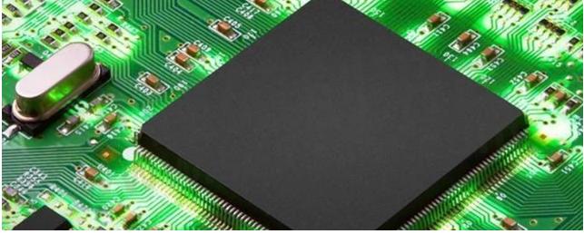
Fig.1
According to the difference in bandgap width, semiconductor materials can be divided into the following four generations.
1. The first generation of semiconductor materials is represented by elemental semiconductor materials such as silicon and germanium. Its typical application is integrated circuits, mainly used in low voltage, low frequency, low power transistors and detectors.
2. The second generation semiconductor materials are represented by gallium arsenide and indium phosphide (InP). The electron mobility of gallium arsenide material is 6 times that of silicon and has a direct band gap. Therefore, its devices have high-frequency and high-speed optoelectronic properties compared to silicon devices, and it is recognized as a very suitable semiconductor material for communications. At the same time, its application in military electronic systems is becoming increasingly widespread and irreplaceable.
3. The third generation semiconductor materials refer to Group III nitrides (such as gallium nitride (GaN), aluminum nitride (AlN), etc.), silicon carbide, oxide semiconductors (such as zinc oxide (ZnO), gallium oxide (Ga2O3), calcium Wide bandgap semiconductor materials such as titanium (CaTiO3), etc.) and diamond. Compared with the first two generations of semiconductor materials, the third generation of semiconductor materials has a large bandgap and superior properties such as a high breakdown electric field, high thermal conductivity, high electron saturation rate, and strong radiation resistance.
4. The fourth generation semiconductor refers to ultra-wideband gap semiconductor materials such as gallium oxide (Ga2O3), diamond (C), and aluminum nitride (AlN), as well as ultra-narrow band gap semiconductors such as gallium antimonide (GaSb) and indium antimonide (InSb).
Features
Compared with the first and second generation semiconductors, the third generation semiconductors have the characteristics of high power, high frequency, high pressure, and high temperature resistance, and are ideal for use in emerging fields such as new energy vehicles, 5G base stations, photovoltaic energy storage, and data centers. Material.
Compared with silicon-based devices, power devices made of silicon carbide materials show better physical properties in high-voltage scenarios and have been widely used in new energy vehicle inverters and photovoltaic inverters.
Gallium nitride materials can be made into power, radio frequency, and optoelectronic devices, depending on their epitaxial layer structure. Gallium nitride power devices often use silicon substrates, and are now widely used in the consumer charger market; radio frequency devices mostly use silicon carbide materials as substrates, which are very suitable for 5G base stations, military radars, and other scenarios; in terms of optoelectronic devices, sapphire substrates are used LEDs made of gallium nitride are already very mature.
Development Trends
●Silicon carbide substrate can be used to prepare silicon carbide power devices and gallium nitride radio frequency devices and is regarded as the core raw material of the third generation semiconductor. However, it is currently limited by the PVT growth method, which makes mass production very difficult. Manufacturers such as Wolfspeed are promoting 6 inches to 8 inches. In addition, emerging growth methods such as liquid phase methods are also developing.
●Compared with optoelectronics and radio frequency applications, the gallium nitride power market has just started. It is transitioning from consumer electronics to industrial fields such as data centers and photovoltaic energy storage, and then entering the automotive market. The future development prospects are huge.
- |
- +1 赞 0
- 收藏
- 评论 0
本文由三年不鸣转载自Yint News,原文标题为:What Is The Third Generation Semiconductor?,本站所有转载文章系出于传递更多信息之目的,且明确注明来源,不希望被转载的媒体或个人可与我们联系,我们将立即进行删除处理。
相关推荐
SIC MOS管栅极问题思考与解决
2025年4月 - 技术文档 本文探讨了SIC MOS管栅极损坏的原因及保护措施。文章首先介绍了SIC MOS管的发展与现状,随后详细分析了栅极容易损坏的原因,包括寄生电容、过电压、高温环境和制造工艺缺陷等。最后,文章提出了使用瞬态抑制二极管(如SMBJ1505CA)来保护栅极,提高其可靠性和稳定性。
音特电子 - SIC MOS管,智能电网,新能源汽车,光伏

当前世界GaN的应用发展情况介绍
2024-06-27 - 行业资讯 面对GaN在消费电子领域应用现状,相关企业开始寻求新的增量市场,GaN技术应用由此逐步向新能源汽车、光伏、数据中心等其他应用场景延伸。GaN的特殊价值,正在消费电子之外的多个领域持续释放。
碳化硅的特性和发展历史简要
2023-11-24 - 行业资讯 碳化硅(Silicon Carbide,简称SiC)是一种广泛应用于半导体、电力电子器件和耐高温材料的材料。本文是碳化硅的特性和发展历史的简要概述。

What Is A Power Semiconductor Device?
2023-08-18 - 技术探讨 Power semiconductor components are semiconductor components used for power control belonging to analog semiconductors, usually called power devices, including rectifier diodes, power transistors (power MOSFET, IGBT), thyristors, and gates. About GTOs, triacs, etc.

What Is Ion Implantation Of Silicon Carbide?
2023-07-11 - 技术探讨 Ion implantation of silicon carbide is a technique used to introduce specific impurity atoms in silicon carbide materials.Ion implantation typically implants desired dopants into silicon carbide crystals by means of a high-energy ion beam.

音特电子推出体积更小的GaN Protect功率保护器件,可实现比传统硅器件芯片2.7~3倍的充电速度
2023-04-24 - 原厂动态 GaN Protect氮化镓将多种电力电子器件整合到一个氮化镓芯片上,能有效提高产品充电速度、效率、可靠性和成本效益。GaN氮化镓是提高整个系统性能的关键,是创造出接近“理想开关”的电路构件,即一个能将最小能量的数字信号,转化为无损功率传输的电路构件。

至信微电子碳化硅肖特基二极管选型表
选型表 - 至信微电子 至信微电子提供碳化硅肖特基二极管选型,涵盖650V、1200V、1700V、2000V等多种电压等级,正向电流IF覆盖2A至100A,具备低正向压降VF(1.25V–1.7V)、高浪涌电流IFSM(12A–900A)与低反向恢复电荷Qc(3.7nC–738nC)。产品系列包括T2、T3、J、D88、D56、F2、NAS、DAS等多种型号,散热能力强(Ptot 31W–600W),适用于高频开关电源、光伏逆变器、PFC电路、工业电机驱动及新能源汽车电控等高效能场景。
|
产品型号
|
品类
|
VRRM
|
IF
|
IFSM
|
VF
|
Ptot
|
Qc
|
|
SDC08065F2AS
|
SiC Schottky Diode
|
650V
|
8A
|
55A
|
1.3V
|
93W
|
23nC
|

LED power supply enters Gan era!
2025-12-02 - 应用方案 The article discusses how gallium nitride (GaN) is transforming LED power supply design by enabling high-frequency, high-efficiency performance that reduces both volume and heat, making it ideal for high-end lighting applications.

Understanding the Benefits of GaN Technology in Power Supplies
2025-10-30 - 技术探讨 GaN technology has emerged as a transformative force in power supply design, offering numerous benefits over traditional silicon-based semiconductors. With its superior electron mobility, thermal characteristics, and ability to operate at higher frequencies, GaN enables engineers to create power supplies that are not only more efficient but also significantly smaller in size.

ROHM and TSMC Launch Strategic Gallium Nitride Technology Collaboration for Automotive Industry
2024-12-12 - 原厂动态 ROHM and TSMC have entered a strategic partnership on development and volume production of gallium nitride (GaN) power devices for electric vehicle applications.

Central Semiconductor Announces New GaN FETs in a Variety of Packages, for Soft Switching Applications with High Efficiency
2024-11-01 - 原厂动态 Central Semiconductor announces the introduction of several new GaN FETs. The latest additions include the CCSPG1060N, the CDF56G6511N, and the CDF56G6517N.


What are the main characteristics of silicon carbide? Why does silicon carbide perform better than IGBT at high frequencies?
2024-10-10 - 技术探讨 Silicon carbide (SiC) is a semiconductor compound composed of silicon (Si) and carbon (C), belonging to the wide bandgap (WBG) material family. Its physical bonds are very strong, giving semiconductors high mechanical, chemical, and thermal stability. The wide bandgap and high thermal stability enable SiC devices to be used at junction temperatures higher than silicon, even exceeding 200 ° C. The main advantage of silicon carbide in power applications is its low drift region resistance, which is a key factor in high-voltage power devices. Today, let‘s share 10 things about gallium nitride

SMD1812-010-60V
2026/02/04 - 数据手册 本资料主要介绍了SMD1812-010-60V型号的过电流保护器件,包括其性能参数、测试条件、焊接条件、存储条件和注意事项。
音特电子 - 过电流保护器件 (PPTC),SMD1812-010-60V,适用于各种电子设备中的过电流保护
SMD1812-014-60V
2026/02/04 - 数据手册 本资料详细介绍了SMD1812-014-60V型号的过电流保护器件,包括其性能参数、测试条件、焊接条件、存储条件和注意事项。
音特电子 - 热敏电阻保护器 (PPTC),SMD1812-014-60V,过电流和过温保护

电子商城

现货市场

授权代理品牌:集成电路


授权代理品牌:分立元件


授权代理品牌:接插件及结构件


授权代理品牌:部件、组件及配件


授权代理品牌:电源及模块


授权代理品牌:电子材料


授权代理品牌:仪器仪表及测试配组件


授权代理品牌:电工工具及材料


授权代理品牌:机械电子元件


授权代理品牌:加工与定制


登录 | 立即注册
提交评论